Section13.7A Brief Introduction to Switching Theory and Logic Design
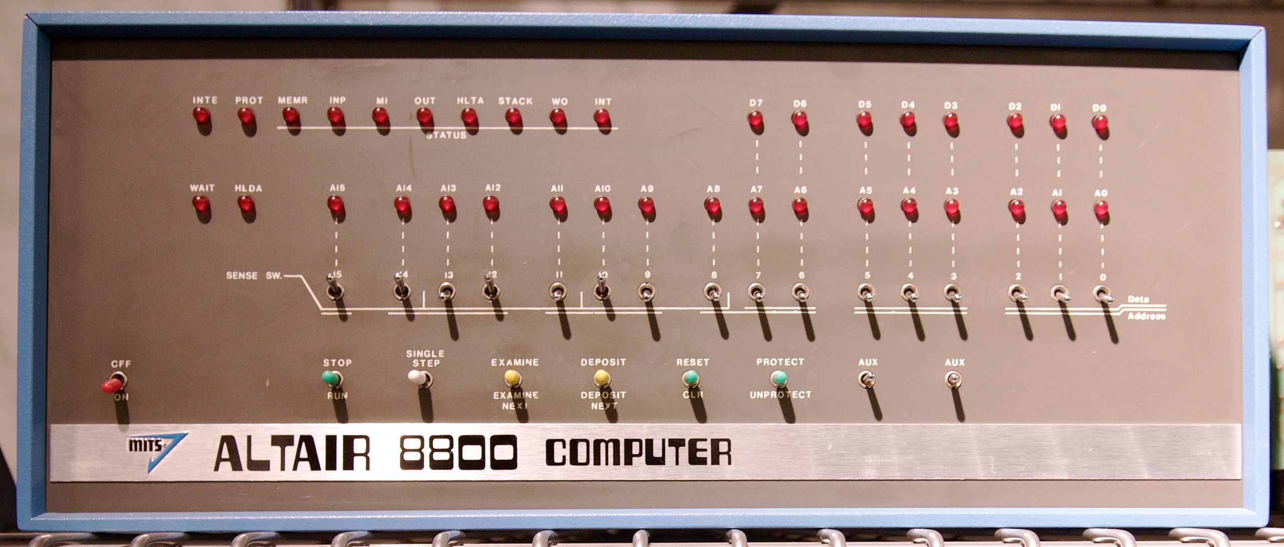
Early computers relied on many switches to perform the logical operations needed for computation. This was true as late as the 1970’s when early personal computers such as the Altair ( Figure 13.7.1) started to appear. Pioneering computer scientists such as Claude Shannon realized that the operation of these computers could be simplified by making use of an isomorphism between computer circuits and boolean algebra. The term Switching Theory was used at the time. Logical gates realized through increasingly smaller and smaller integrated circuits still perform the same functions as in early computers, but using purely electronic means. In this section, we give examples of some switching circuits. Soon afterward, we will transition to the more modern form of circuits that are studied in Logic Design, where gates replace switches. Our main goal is to give you an overview of how boolean functions corresponds to any such circuit. We will introduce the common system notation used in logic design and show how it corresponds with the mathematical notation of Boolean algebras. Any computer scientist should be familiar with both systems.
Figure13.7.1.The Altair Computer, an early PC, by Todd Dailey, Creative Commons
The simplest switching device is the on-off switch. If the switch is closed/ON, current will pass through it; if it is open/OFF, current will not pass through it. If we designate ON by 1, and OFF by 0, we can describe electrical circuits containing switches by Boolean expressions with the variables representing the variable states of switches or the variable bits passing through gates.
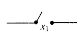
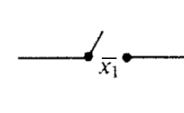
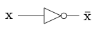
The electronics involved in these switches take into account whether we are negating a switch or not. For electromagnetic switches, a magnet is used to control whether the switch is open or closed. The magnets themselves may be controlled by simple ON/OFF switches. There are two types of electromagnetic switches. One is normally open (OFF) when the magnet is not activated, but activating the magnet will close the circuit and the switch is then ON. A separate type of switch corresponds with a negated switch. For that type, the switch is closed when the magnet is not activated, and when the magnet is activated, the switch opens. We won’t be overly concerned with the details of these switches or the electronics corresponding to logical gates. We will simply assume they are available to plug into a circuit. For simplicity, we use the inversion symbol on a variable that labels a switch to indicate that it is a switch of the second type, as in Figure 13.7.3.
Figure13.7.2.Representation of a normally OFF switch controlled by variable \(x_1\)
Figure13.7.3.Representation of a normally ON switch controlled by variable \(x_1\)
The standard notation used for Boolean algebra operations in switching theory and logic design is \(+\) for join, instead of \(\lor \text{;}\) and \(\cdot \) for meet, instead of \(\land \text{.}\) Complementation is the same in both notational systems, denoted with an overline.
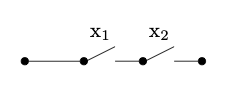
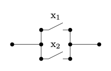
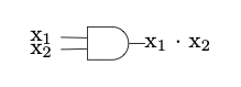
The expression \(x_1 \cdot x_2\) represents the situation in which a series of two switches appears in sequence as in Figure 13.7.4. In order for current to flow through the circuit, both switches must be ON; that is, they must both have the value 1. Similarly, a pair of parallel switches, as in Figure 13.7.5, is described algebraically by \(x_1 + x_2\text{.}\) Here, current flows through this part of the circuit as long as at least on of the switches is ON.
Figure13.7.4.Two switches in AND configuration realizing \(x_1 \cdot x_2\)
Figure13.7.5.Two switches in OR configuration realizing \(x_1 + x_2\)
All laws and concepts developed previously for Boolean algebras hold. The only change is purely notational. We make the change in this section solely to introduce the reader to another frequently used system of notation.
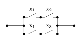
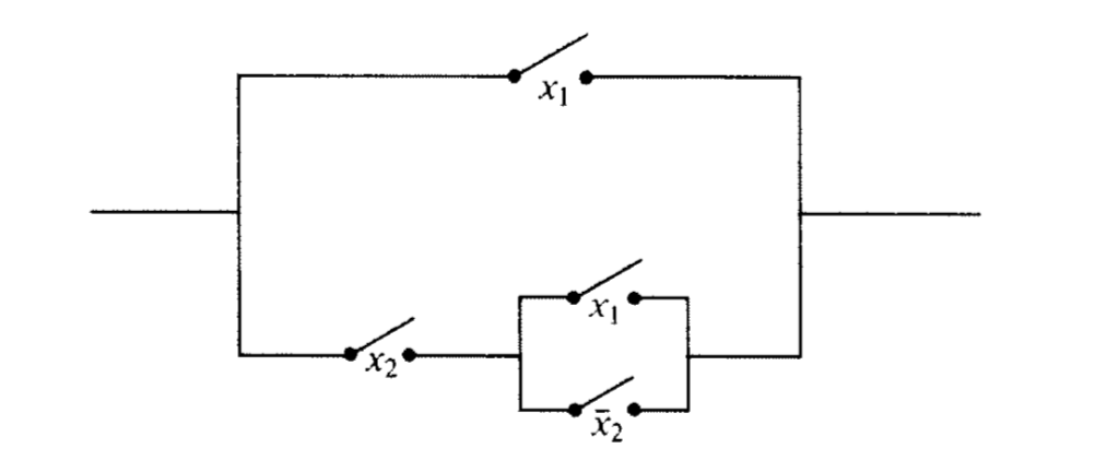
Many of the laws of Boolean algebra can be visualized thought switching theory. For example, the distributive law of meet over join is expressed as
The switching circuit analogue of the above statement is that the circuits in the two images below are equivalent. In circuit (b), the presence of two \(x_1\)’s might represent two electromagnetic switches controlled by the same magnet.
Figure13.7.6.(a)
Figure13.7.7.(b)
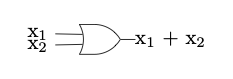
The circuits in a computer are now composed of large quantities of gates, which serve the same purpose as switches, but can be miniaturized to a great degree. For example, the OR gate, usually drawn as in Figure 13.7.8 implements the logical OR function. This happens electronically, but is equivalent to Figure 13.7.5. The AND gate, which is equivalent to two sequential switches is shown in Figure 13.7.8.
Figure13.7.8.An OR gate
Figure13.7.9.An AND gate
The complementation process is represented in a gate diagram by an inverter, as pictured in Figure 13.7.10.
Figure13.7.10.Inverter, or NOT gate
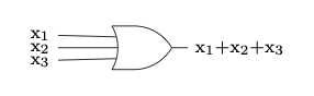
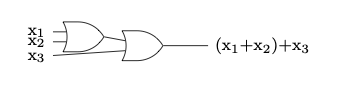
When drawing more complex circuits, multiple AND’s or OR’s are sometimes depicted using a more general gate drawing. For example if we want to depict an OR gate with three inputs that is ON as long as at least one input is ON, we would draw it as in Figure 13.7.11, although this would really be two binary gates, as in Figure 13.7.12. Both diagrams are realizing the boolean expression \(x_1 + x_2 + x_3\text{.}\) Strictly speaking, the gates in Figure 13.7.12 represent \((x_1 + x_2 )+ x_3\text{,}\) but the associative law for join tells us that the grouping doesn’t matter.
Figure13.7.11.Simple version of a ternary OR gate
Figure13.7.12.A ternary OR gate created with binary OR gates
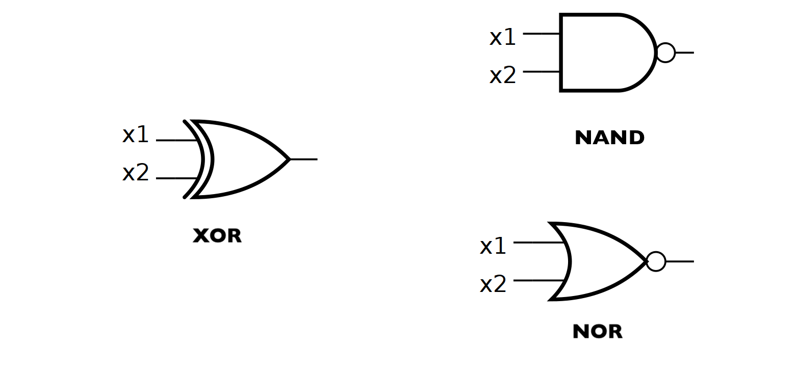
In Figure 13.7.13, we show a few other commonly used gates, XOR, NAND, and NOR, which correspond to the boolean exressions \(x_1 \oplus x_2\text{,}\)\(\overline{x_1 \cdot x_2}\text{,}\) and \(\overline{x_1 + x_2}\text{,}\) respectively.
Figure13.7.13.Other common gates
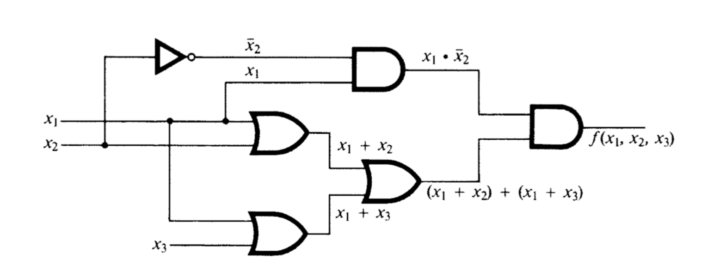
Let’s start with a logic circuit and see how the laws of boolean algebra can help us simplify it.
We simplify the boolean expression that defines \(f\text{,}\) simplifying the circuit in so doing. You should be able to identify the laws of Boolean algebra that are used in each of the steps. See Exercise 13.7.1.
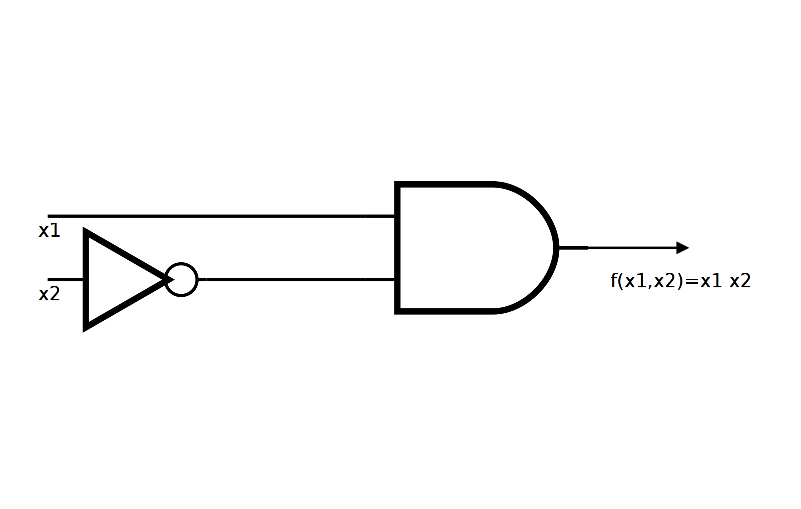
Therefore, \(f\left(x_1, x_2, x_3\right)=x_1 \cdot \overline{x_2}\text{,}\) which can be realized with the much simpler circuit in Figure 13.7.16, without using the input \(x_3\text{.}\)
Figure13.7.16.Simplified gate diagram
Next, we start with a table of desired outputs based on three bits of input and design an efficient circuit to realize this output.
Consider the following table of desired outputs for the three input bits \(x_1, x_2, x_3\text{.}\)
Table13.7.18.Desired output table
\(x_1\)
\(x_2\)
\(x_3\)
\(f(x_1,x_2,x_3)\)
0
0
0
0
0
0
1
1
0
1
0
0
0
1
1
0
1
0
0
1
1
0
1
1
1
1
0
0
1
1
1
0
The first step is to write the Minterm Normal Form of \(f\text{.}\) Since we are working with the two value Boolean algebra, \(B_2\text{,}\) the constants in each minterm are either 0 or 1, and we simply list the minterms that have a 1. These correspond with the rows of the table above that have an output of 1. We will then attempt to simplify the expression as much as possible.
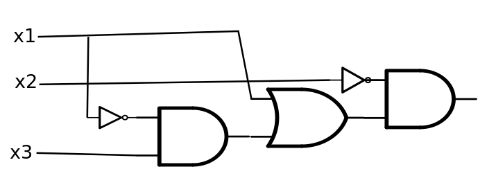
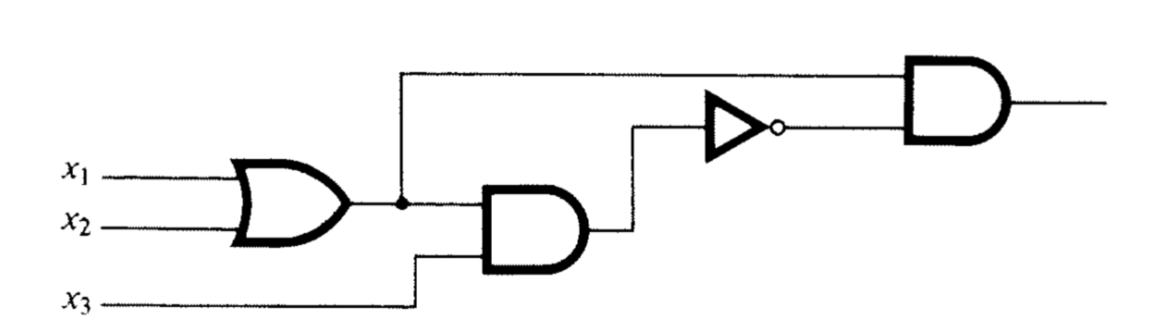
Therefore we can realize our table with the boolean function \(f\left(x_1, x_2, x_3\right)=\overline{x_2} \cdot ((\overline{x_1} \cdot x_3) + x_1)\text{.}\) A circuit diagram for this function is Figure 13.7.19. But is this the simplest circuit that realizes the table? See Exercise 13.7.3.
Figure13.7.19.A realization of the table of desired outputs.
ExercisesExercises
1.
List the laws of boolean algebra that justify the steps in the simplification of the boolean function \(f\left(x_1, x_2, x_3\right)\) in Example 13.7.14. Some steps use more than one law.
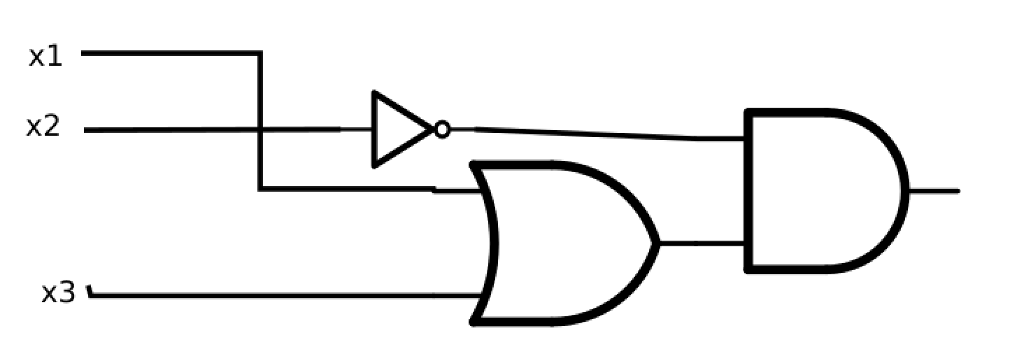
Trace the inputs though this circuit and determine the Boolean function that it realizes.
Construct a table of outputs for each of the eight inputs to this circuit.
Find the minterm normal form of \(f\text{.}\)
Draw the circuit based on the minterm normal form.
Simplify the circuit algebraically and draw the resulting circuit.
6.
Consider the Boolean function \(f\left(x_1, x_2, x_3, x_4\right)=x_1 + \left(x_2 \cdot \left(\overline{x_1} + x_4\right) + x_3 \cdot \left(\overline{x_2} + \overline{x_4}\right)\right).\)
Simplify \(f\) algebraically.
Draw the gate diagram based on the simplified version of \(f\text{.}\)
7.
Draw a logic circuit using only AND, OR and NOT gates that realizes an XOR gate.
8.
Draw a logic circuit using only AND, OR and NOT gates that realizes the Boolean function on three variables that returns 1 if the majority of inputs are 1 and 0 otherwise.