Dan Wasserman

| Department of Physics and Applied Physics


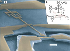
Image showing device structure of Nanometre-scale displacement sensing using a single electron transistor, Robert G. Knobel and Andrew N. Cleland, Nature 424, 291-293(17 July 2003)


F2008: Solid State Electronics and Optoelectronic Devices

General Information:
 Syllabus

Lecture Notes/Images:

Lecture 1: The Crystalline State (9/3/08)

Lecture 5: The Kronig-Penney Model

Lecture 7: Semiconductor Band Structure

Lecture 17: Rectifying Diode


Homework

Homework 1 (due 9/10/08)

Homework 1 Solutions

Homework 2 (due 9/24/08)

Homework 2 Solutions

Homework 3 (due 10/1/08)

Homework 3 Solutions

Homework 4 (due 10/8/08)

Homework 4 Solutions

Homework 5 (due 10/15/08)

Homework 5 Solutions

Homework 6 (Mid-Term Exam)

Mid Term Exam 1 Solutions

Homework 7 (due 11/12/08)

Homework 7 Solutions

Homework 8(due 11/19/08)

Homework 8 solutions

Midterm #2 and Solutions

Homework #9 (due 12/3/08)

Homework #10 (due 12/10/08)


Instructor Evaluation Form

F2008 Evaluation